New Canon Option for Semiconductor Lithography System Back-end Process Contributes to 3D Advanced Packaging Technologies, Enables Mass Production of Dense Circuitry with Exposure Fields of Up to 100 mm x 100 mm
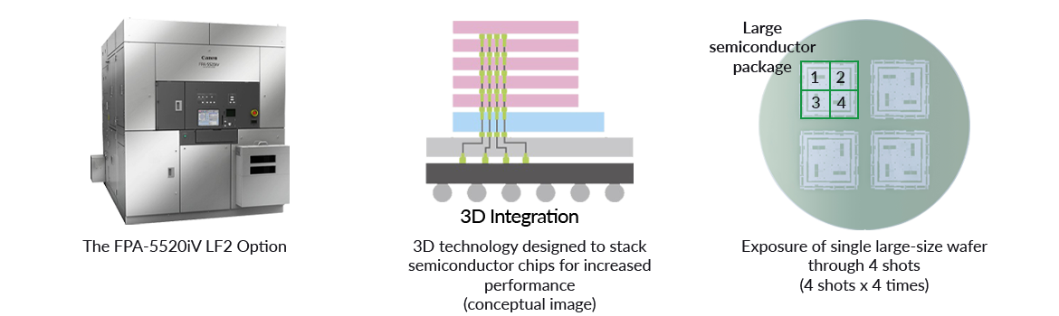
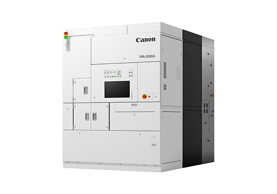
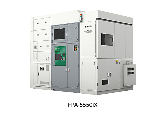
SINGAPORE, 6 December 2022 — Canon Inc. announced today the launch in Japan of the FPA-5520iV LF2 Option for back-end process semiconductor lithography i-line stepper1 systems that contributes to 3D advanced packaging technologies with a 0.8 µm (micrometer2) resolution and a wide exposure field of 100 mm x 100 mm.
In the field of semiconductor chip performance enhancement, alongside miniaturization of circuits in front-end process of semiconductor manufacturing, higher-density packaging in back-end processes is attracting greater attention. Advanced packaging that realizes high performance requires fine rewiring, and in recent years, semiconductor lithography systems have been used for this purpose. There is a growing need for increasing semiconductor performance through “2.5D technology3” in which semiconductor chips are integrated with extremely high die-to-die interconnect density, as well as “3D technology4”, in which active chips are integrated by die stacking for the shortest interconnect and smallest package footprint. The new FPA-5520iV LF2 Option features a high resolution of 0.8 µm and 4-shot exposure with minimal distortion to make possible a wide exposure field of 100 mm x 100 mm. This in turn enables mass production of large and dense packaging with circuit patterns that integrate 2.5D and 3D technology.
The new FPA-5520iV LF2 Option reduces distortion aberration of less than 1/4 that of its predecessor model, the FPA-5520iV LF Option (released in April 2021), and features a new projection optical system with greater light level uniformity. These advancements allow LF2 Option steppers to provide 0.8 µm resolution across a large 52 mm × 68 mm single-exposure field at while also making possible an ultra-wide 100 mm x 100 mm exposure field.
The FPA-5520iV LF2 Option inherits the basic performance of the FPA-5520iV, which has the ability to handle warped reconstituted substrates5 an issue which can occur in packaging layers during the mass-production process, as well as high productivity to enhance availability by detecting alignment marks—even on the reconstituted substrates with large chip array variations.
Going forward, Canon will strive to support further technological innovation by expanding its lineup of semiconductor lithography system offerings not only for front-end semiconductor chip manufacturing processes, but also systems that support state-of-the-art back-end packaging technologies.
About Canon Singapore Pte. Ltd.
Canon is a global leader in photographic and digital imaging solutions. Canon Singapore Pte. Ltd. is the headquarters for South & Southeast Asia driving sales, marketing and service strategies. Besides handling the domestic market, the company covers 22 other countries and regions including subsidiaries in India, Malaysia, Thailand and Vietnam. The parent company Canon Inc. has a global network of more than 300 companies and employs about 180,000 people worldwide. Canon is guided by its kyosei philosophy that focuses on living and working together for the common good.
More information is available at https://sg.canon.
1 A semiconductor lithography system that utilizes a 365 nm wavelength mercury lamp as the light source. 1 nm (1 nanometer) = 1 billionth of a meter.
2 1 µm (1 micrometer) = one millionth of a meter = one thousandth of a millimeter.
3 Packaging to combine different chips. The chips can be placed close together and connected electrically by a number of circuits to increase processing capability.
4 Refers to Through Silicon Via (TSV) technology, where memory chips are stacked to achieve high capacity.
5 Wafers created by attaching and encasing in resin multiple individual semiconductor chips that are produced during the front-end processes of semiconductor manufacturing.