Canon Releases FPA-3030i6 Semiconductor Lithography System for Small Wafers
Canon Releases FPA-3030i6 Semiconductor Lithography System for Small Wafers
With a newly developed lens and a variety of options to meet the growing demand for power devices
SINGAPORE, 26 September 2024 — Canon Inc. announced on 24 September the release of the FPA-3030i6 i-line1 stepper, a new semiconductor lithography system for processing wafers with a diameter of 8 inches (200 mm) or smaller.
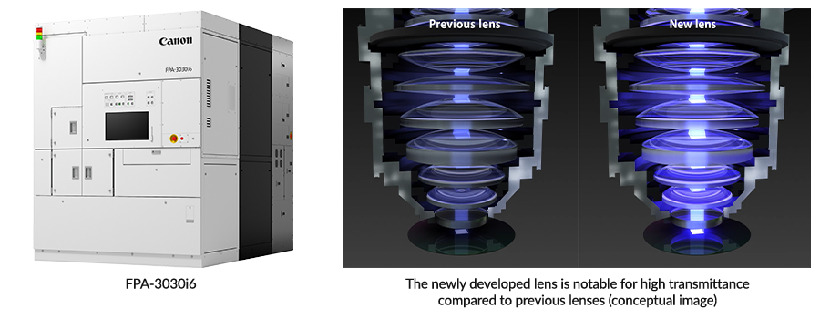
The FPA-3030i6 employs a newly developed projection lens that boasts high transmittance and high-durability. The system reduces lens aberration for high exposure dose processes and improves productivity by shortening exposure time.
The lens is made of high-transmittance glass material that reduces lens aberrations occurring during exposure by more than 50%2 when compared to previous stepper models3. Higher transmittance also helps reduce exposure time while maintaining pattern fidelity, even under high exposure dose conditions.
Improving lens transmittance will also increase exposure intensity and shorten the exposure time required for each process. The FPA-3030i6 standard productivity for 8 inch (200 mm) wafers has increased4 to 130 wafers per hour from 123 for the previous stepper models.
Additionally, since the lens is highly durable, lens transmittance decrease over time is reduced and productivity can be maintained over the life of the system.
The NA (numerical aperture) range has also been expanded from 0.45~0.63 in the previous model to 0.30~0.63. Allowing for a smaller NA enables customers to select the optimum NA for each device layer.
Optional products including a wafer handling system for special substrates are available for order to meet users’ manufacturing needs for various emerging semiconductor devices including high-power and high-efficiency green devices.
The FPA-3030i6 is designed to support a wider range of device fabrication thanks to a variety of available process options for silicon (Si) as well as sapphire and compound semiconductor materials such as silicon carbide (SiC), gallium nitride (GaN) and gallium arsenide (GaAs) substrates.
Canon will offer wafer feeding options enabling handling of substrates from 2 inches (50 mm) to 8 inches (200 mm) in diameter, as well as thick, thin and warped substrate handling.
About Canon Singapore Pte. Ltd.
Canon is a global leader in photographic and digital imaging solutions. Canon Singapore Pte. Ltd. is the headquarters for South & Southeast Asia driving sales, marketing and service strategies. Besides handling the domestic market, the company covers 22 other countries and regions including subsidiaries in India, Malaysia, Thailand and Vietnam. The parent company Canon Inc. has a global network of more than 300 companies and employs about 169,000 people worldwide. Canon is guided by its kyosei philosophy that focuses on living and working together for the common good.
More information is available at https://sg.canon.
1 Semiconductor lithography equipment using i-line (Mercury lamp, wavelength 365 nm) light source 1 nm (nanometer) = 1/1 billion meter.
2 Under Canon's standard exposure conditions.
3 FPA-3030i5a (released in March 2021).
4 8 inch (200 mm) wafer.
