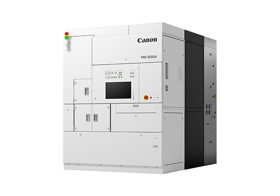
Nanoimprint Lithography Semiconductor Manufacturing System that Covers Diverse Applications with Simple Patterning Mechanism
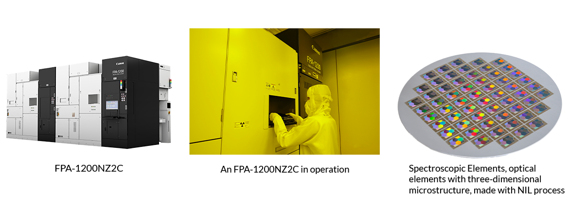
SINGAPORE, 31 October 2023 — Canon announced today the launch of the FPA-1200NZ2C nanoimprint semiconductor manufacturing equipment, which executes circuit pattern transfer, the most important semiconductor manufacturing process.
By bringing to market semiconductor manufacturing equipment with nanoimprint lithography (NIL) technology, in addition to existing photolithography systems, Canon is expanding its lineup of semiconductor manufacturing equipment to meet the needs of a wide range of users by covering from the most advanced semiconductor devices to the existing devices.
In contrast to conventional photolithography equipment, which transfers a circuit pattern by projecting it onto the resist coated wafer, the new product does it by pressing a mask imprinted with the circuit pattern on the resist on the wafer like a stamp. Because its circuit pattern transfer process does not go through an optical mechanism, fine circuit patterns on the mask can be faithfully reproduced on the wafer. Thus, complex two- or three- dimensional circuit patterns can be formed in a single imprint1, which may reduce the cost of ownership (CoO).
Canon's NIL technology enables patterning with a minimum linewidth of 14 nm2, equivalent to the 5-nm-node3 required to produce most advanced logic semiconductors which are currently available. Furthermore, with further improvement of mask technology, NIL is expected to enable circuit patterning with a minimum linewidth of 10 nm, which corresponds to 2-nm-node.
The new product employs newly developed environment control technology that suppresses the contamination with fine particles in the equipment.
This enables high-precision alignment which is necessary for the manufacture of semiconductors with an increasing number of layers and the reduction of defects due to fine particles, and enables the formation of fine and complex circuits, contributing to the manufacture of cutting-edge semiconductor devices.
Since the new product does not require a light source with a special wavelength for fine circuit, it can reduce power consumption significantly compared to the photolithography equipment for currently available most advanced logic semiconductors (5-nm-node with 15 nm linewidth), thereby contributing to CO2 reduction.
The new product can be used for a wide range of applications, such as metalenses4 for XRs with microstructures of tens of nanometers, in addition to logic and other semiconductor devices.
About Canon Singapore Pte. Ltd.
Canon is a global leader in photographic and digital imaging solutions. Canon Singapore Pte. Ltd. is the headquarters for South & Southeast Asia driving sales, marketing and service strategies. Besides handling the domestic market, the company covers 22 other countries and regions including subsidiaries in India, Malaysia, Thailand and Vietnam. The parent company Canon Inc. has a global network of more than 300 companies and employs about 180,000 people worldwide. Canon is guided by its kyosei philosophy that focuses on living and working together for the common good.
More information is available at https://sg.canon.
1 A pattern forming process of nanoimprinting.
2 One billionth of a meter.
3 “nm-node”: a generation of semiconductor technology.
4 An element with the same function as a lens by controlling light with a fine structure smaller than the wavelength of visible light.